List of Ongoing Research Projects
- CAD Tools for Multi-Objective Multicore Architecture Design
- Design for Emerging Memory Architectures
List of Past Research Projects
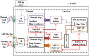
Silicon Photonics for Multicore Computing
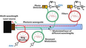
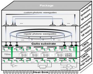
Enabling high bandwidth and power-efficient communication between information processing cores in System-on-Chip (SoC) architectures is an essential but increasingly difficult aspect of electronic chip design. SoCs play a pivotal role in society today, as these application-specific high-performance VLSI circuits drive all major modern inventions including vehicles and airplanes, computers and phones, scientific and industrial infrastructure, as well as military systems. With SoC processing core counts increasing steadily every year to enable more sophisticated applications (e.g., high fidelity target discrimination, warfighter control and navigation), the demands of higher bandwidth and low latency transfers are putting greater pressure on SoC communication networks. The result is that chip power and performance are now dominated not by processor cores but by the network that transports data between processors and to memory. In other words, SoC robustness and quality is now network dominated. The research objective of this project is to determine the best architectural modalities to insert silicon photonic interconnect technology into electronic chips, in order to overcome performance and energy bottlenecks in today’s SoCs. The project involves creating performance, energy, and reliability models, circuits, architectures, and optimization techniques, to expedite the deployment of silicon photonics into manycore SoCs in the near future, to overcome the severe shortcomings of electrical interconnects at the chip-scale.
Cross-Layer Design of Interconnection Networks-on-Chip
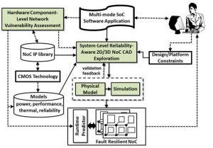
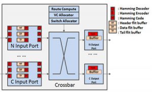
Shrinking feature sizes and the increasing proliferation of mixed-signal and 3D integration are elevating rates of faults, variation, and aging related degradation in integrated circuits, threatening the reliability of communication between cores in system-on-chip (SoC) architectures. It is well known that performance for most SoCs today is interconnect-limited and the design of a high performance network-on-chip (NoC) will become a crucial step as core counts increase from tens today to hundreds in the near future, and 3D die stacking becomes the norm. But the NoC is a key component for another reason: it constitutes a single point of failure on a chip. Mechanisms for fault detection and recovery are thus vital for NoCs, especially in 3D ICs where greater thermal stress due to higher temperatures and thermal cycling accelerates a multitude of degradation affects, increasing transient and permanent fault rates at runtime. Unfortunately, current techniques to ensure NoC reliability at runtime, including fault tolerant routing, and architectural solutions operate at only one level of the system stack. Such single-layer techniques possess limited knowledge of application execution activity, and are therefore reactive in behavior, making worst-case assumptions about other layers. As a result, they introduce significant power, area, and performance overheads during typical-case operation for corner-case errors that occur very infrequently. The research objective of this project is to realize a multi-objective computer-aided design (CAD) automation framework at the system-level, where design decisions have the most impact, to assist chip designers trade-off reliability with competing design constraints within tight time-to-market constraints. This framework is novel as it will exploit cross-layer insights about the software application, hardware IP blocks, and circuits, as well as knowledge of key factors impacting susceptibility to runtime faults for NoC routers and interfaces. The research aims to create novel tools and techniques that will have a significant impact in industry by improving designer productivity and ushering in new levels of cost-efficiency during the reliable-by-construction design of network fabrics for SoCs.
CAD Tools for Multi-Objective Multicore Architecture Design
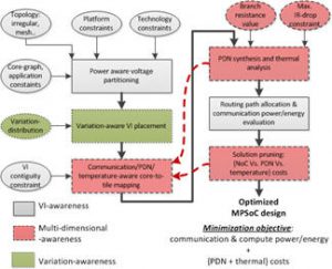
With increasing core counts ushering in power-constrained multiprocessor system-on-chips (MPSoCs), optimizing power dissipated by the computation cores and the network-on-chip (NoC) fabric is critical. At the same time, with increased power densities, especially in 3D ICs, problems of IR drops in the Power Delivery Network (PDN) as well as thermal hot spots on the die are very severe. Additionally, variations in emerging fabrication processes introduce significant unpredictability in system behavior. System-level design approaches that are aware of these challenges are crucial for designing efficient MPSoCs. This project recognizes that for each new configuration of computation core and communication mapping on an MPSoC, the corresponding inter-core communication patterns, 3D on-chip thermal profile, IR-drop distribution in the PDN, as well as impact of process variations on system performance can vary significantly. Based on this key observation, the research objective of this project is to design a novel system-level co-synthesis framework that intelligently maps computation and communication resources on a die to minimize overall system power (including computation, communication and chip-cooling power) and optimize the PDN architecture; while meeting performance goals and satisfying thermal constraints. The project also considers emerging challenges for multicore computing at runtime, such as soft and hard errors, dim and dark silicon, and process/voltage/thermal (PVT) variations.
Design for Emerging Memory Architectures

On-chip memory architectures in multi-core systems can occupy up to 70% of the die area and have a significant impact on system cost, performance, power dissipation, and time-to-market. Off-chip memory is not expected to scale well for high performance computing systems of the future. Designers must therefore carefully explore the memory hierarchy design space to select the appropriate scratchpad memories, caches, SRAM, DRAM, and emerging non-volatile memories to optimize for desired design constraints. The research objective of this project is to investigate the memory requirements of modern parallel applications and understand its interactions with the on-chip communication infrastructure and other components on a manycore chip. The research focus of this exploration is to eventually design new memory components and architectures as well as CAD techniques and tools to assist the designer in optimizing the memory hierarchy for future manycore architectures. The project focuses on 3D stacked DRAM, phase-change RAM (PCRAM), spin-torque RAM (STT-RAM), and memory controller design strategies for high performance, predictable latency, low energy, and high reliability.
System-Level Modeling for Power and Performance Analysis of Multicore SoCs
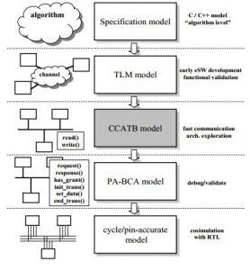
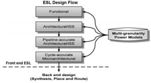
To perform early, system-level exploration of processors, memories, and the on-chip communication architecture, designers require a fast and accurate simulation framework. To address this challenge, the research objective of this project was to design several fast and accurate simulation and estimation frameworks for performance and power evaluation early in the design flow at the system-level. We proposed a novel modeling abstraction called CCATB that allows fast and accurate simulation-based exploration. The CCATB simulation kernel optimally aggregates the delays encountered within a read or write transaction and increments simulation time by multiple cycles wherever possible. This considerably reduces the event scheduling overhead during simulation. The simulation abstraction maintains overall cycle accuracy, while trading off intra-transaction visibility for simulation and modeling speedup. CCATB models of industrial strength MPSoC designs were shown to be more than a 1000X faster than RTL simulation and more than 2X faster than the fastest previously proposed abstraction for communication architecture exploration. Our system-level power modeling framework was shown to be 2000X faster than gate level estimation tools while maintaining more than 95% accuracy.
Design and Exploration of On-Chip Communication Architectures
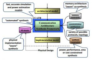
Modern multi-processor system-on-chip (MPSoC) designs are rapidly increasing in complexity, as more and more components are integrated on a single chip. The on-chip communication architecture in such systems must handle the entire inter-component data traffic, and has been shown to have a critical impact on system performance and power consumption. Additionally, the design, customization, exploration and implementation of on-chip communication architectures take up a considerable chunk of the design cycle, affecting time-to-market. These observations motivate the need for a methodology to explore and synthesize on-chip communication architectures earlier in the design flow, at the system level, where design decisions have the greatest impact. To address these requirements, the research objective of this project was to design the COMMSYN framework for automated on-chip communication architecture exploration and synthesis. Unlike existing approaches, COMMSYN enables a physical-implementation aware and memory architecture aware on-chip communication architecture synthesis, comprehensively generating both the topology and parameters (such as clock frequency, data width, arbitration scheme and buffer size), while trading off multiple design constraints such as power, performance, area and cost. Our approach was one of the first to integrate physical floorplan awareness during system-level analysis and exploration. Our memory and communication architecture co-synthesis framework was shown to reduce memory area by as much as 30%, and the number of buses by 40%, compared to traditional approaches where memory and communication architectures are synthesized separately. Our framework to synthesize partial bus matrix communication architectures provided up to a 9X reduction in bus count for complex, industrial strength MPSoC applications, which has significant implications for cost and chip area.
Carbon Nanotube Based On-Chip Interconnect Architectures
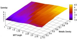
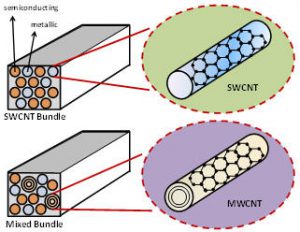
According to the International Roadmap for Semiconductors (ITRS), global interconnect performance has become one of the semiconductor industry’s topmost challenges. Conventional copper (Cu) global interconnects have become increasingly susceptible to electromigration at high current densities (>10^6 A/cm2) leading to considerable degradation in reliability. Additionally, as interconnect dimensions are scaled down, rising crosstalk coupling noise and parasitic resistivity due to electron-surface and grain-boundary scatterings cause global interconnect delay to increase rapidly. There is therefore a critical need to investigate innovative global interconnect alternatives to Cu. Recently, there has been tremendous interest in carbon nanotubes (CNTs) as a possible replacement for Cu interconnects in future technologies. Depending on the direction in which they are rolled (referred to as chirality) CNTs can behave either as semiconductors or conductors. Conducting (or metallic) CNTs possess many extraordinary properties that make them promising candidates for implementing interconnects in UDSM technologies. Due to their covalently bonded structure, they are highly resistant to electromigration and other sources of physical breakdown. They can support very high current densities with very little performance degradation. They also have much better conductivity properties than Cu owing to longer electron mean free path (MFP) lengths in the micrometer range, compared to nanometer range MFP lengths for Cu interconnects. CNTs can be broadly classified into single-walled carbon nanotubes (SWCNTs) and multi-walled carbon nanotubes (MWCNTs). SWCNTs consist of a single sheet of graphene rolled into a cylindrical tube, with a diameter in the nanometer range. MWCNTs consist of two or more SWCNTs concentrically wrapped around each other, with diameters ranging from a few to several hundred nanometers. For on-chip global interconnects, bundles of SWCNTs and mixed SWCNT/MWCNTs are also of special interest because of their superior conductivity properties. An SWCNT bundle consists of several SWCNTs packed together in parallel, whereas a mixed SWCNT/ MWCNT bundle consists of a combination of SWCNTs and MWCNTs packed together in parallel. The research objective of this project was to answer the question: how do CNTs compare against Cu as global interconnect materials? We performed a comprehensive comparative analysis of the performance and energy impact of using CNT-based global interconnects over Cu for heterogeneous multi-core CMP applications. Our experimental results indicated that while SWCNTs are not as suitable for global interconnect buses due to their large ohmic resistance and very high delays, global MWCNT buses can provide performance speedups of up to 1.98× for CMP applications. Global interconnect buses implemented with SWCNT bundles and mixed SWCNT/MWCNT bundles also lead to performance gains over copper global buses of up to 1.3× and 1.5× respectively. These gains can be further improved if the CNT mean free path (MFP) lengths and metallic densities are increased with advances in fabrication technology that are actively being explored today.
Power and Performance Enhancements for Embedded Processors
The research objective of this project was to reduce power and improve performance for embedded microprocessors. We designed novel context-switching aware and skew-based branch predictors that improved processor performance by up to 6% over state of the art branch prediction mechanisms. We also devised novel techniques for dynamically resizing the register file (L2MRFS) which in tandem with dynamic frequency scaling (DFS) significantly improves the performance and reduces energy-delay product for embedded processors. Our approach exploited L2 cache misses, adaptively reducing register file (RF) size during the period when there is no pending L2 cache miss, and using a larger RF during the L2 cache miss period. The RF size adaptation is realized using a circuit modification scheme that comes with minimal hardware modification, unlike costly banking or clustering techniques. Our extensive experimental results show that L2MRFS noticeably improves performance (11% on average) and also significantly reduces energy-delay product (7%) for out-of-order embedded processers.